Matter42
  • Vision
Sign in

Matter42 Atlas

  • Atlas Metrology
  • Atlas Physics AI

Resources

  • Security
  • FAQ
  • Documentation
  • Python SDK

Company

  • Team
  • Careers
  • Blog
Vision
Sign in

The Matter42 vision

Everything we want next is made of something we can’t make yet.

Cooler computers. Sensors that read a single cell. Electronics that survive deep space, speak in light, and bend like paper. Every one of them is waiting on a material.

See what becomes possibleHow we’ll make it

What becomes possible

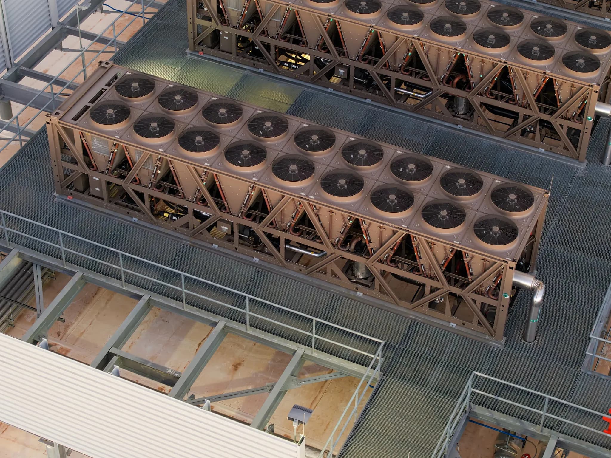
Rows of cooling fans on the roof of a data center.

01 / 06Computing, cooled

Intelligence without the heat.

Devices that switch with a fraction of today’s energy mean data centers that draw less power, shed less heat, and drink less water. AI keeps scaling; the grid doesn’t break.1

Data center cooling · Rsparks3, CC0
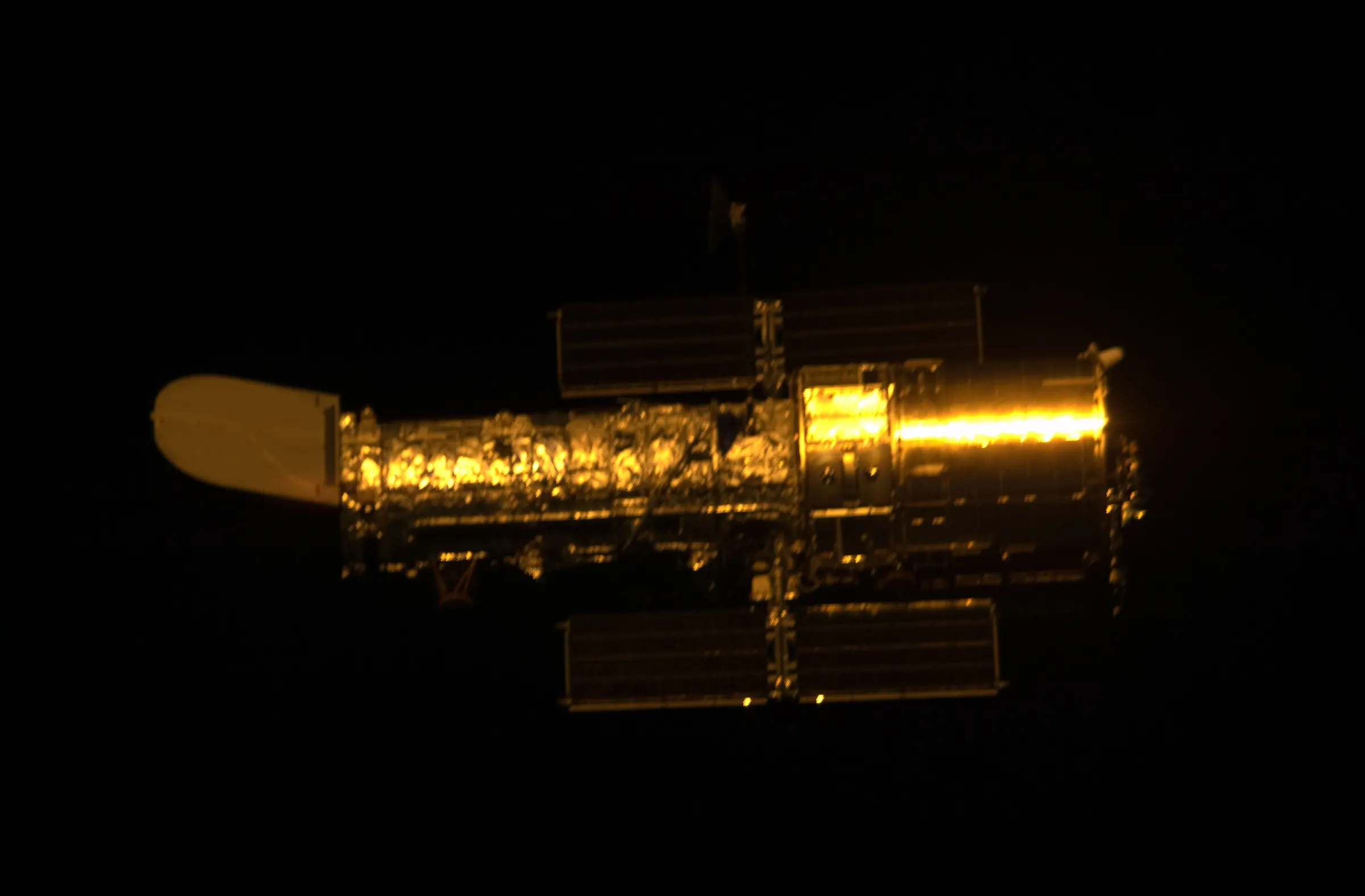
The Hubble Space Telescope drifting in black space after release from Space Shuttle Atlantis.

02 / 06Space

Electronics built for the dark.

A material a few atoms thick gives radiation almost nothing to hit. Lighter satellites, longer missions, and compute in orbit and beyond.2

Hubble after release from Atlantis, 2009 · NASA
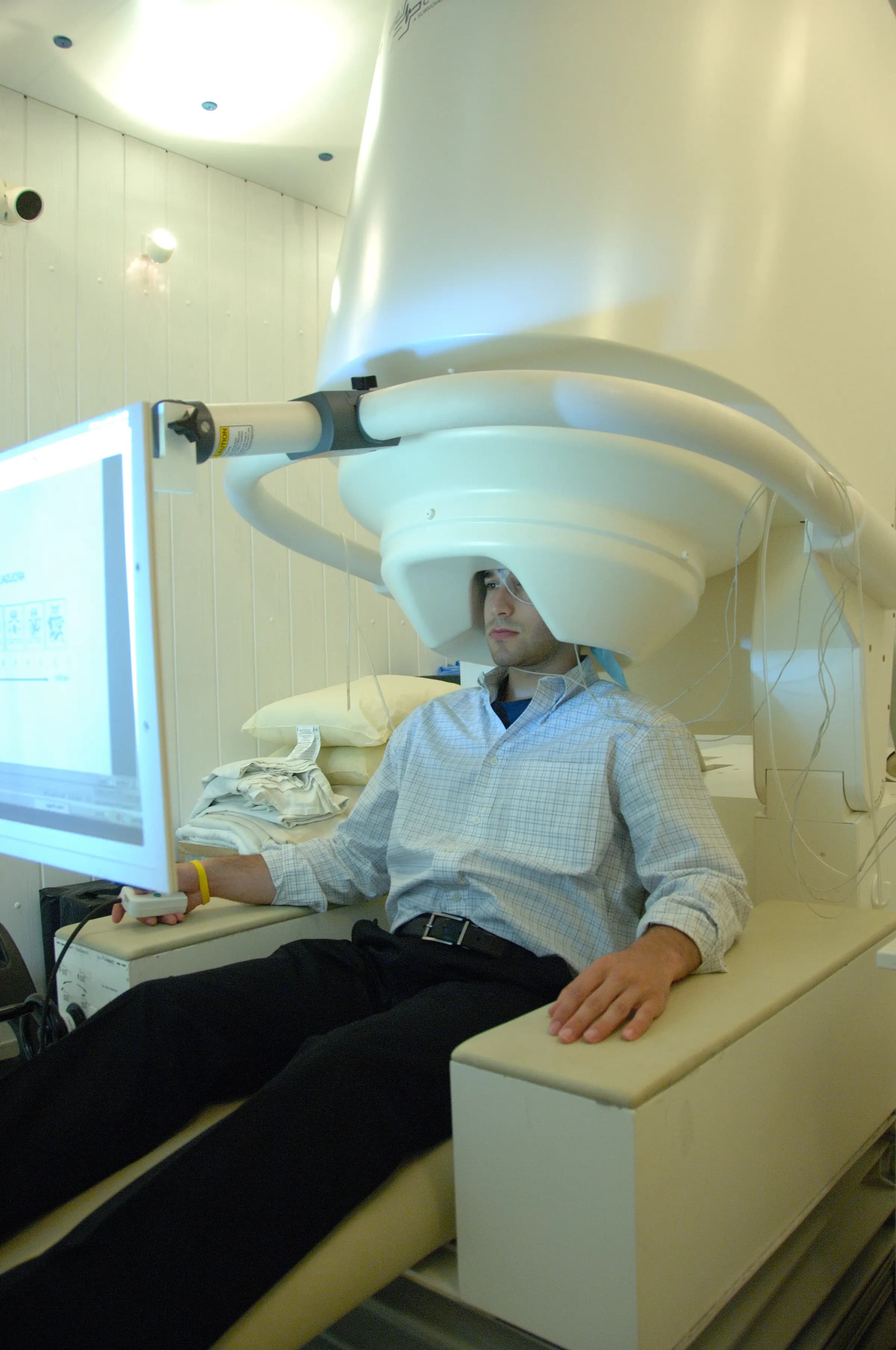
A person seated in a magnetoencephalography scanner that records the brain’s magnetic fields.

03 / 06Medicine

Sensors that see a single cell.

Place one defect on purpose and a crystal becomes a quantum sensor. Only atoms thick, it can sit nanometers from living tissue: toward brain imaging without cryogenics, and magnetic resonance at the scale of a molecule.3

Magnetoencephalography scanner · NIMH
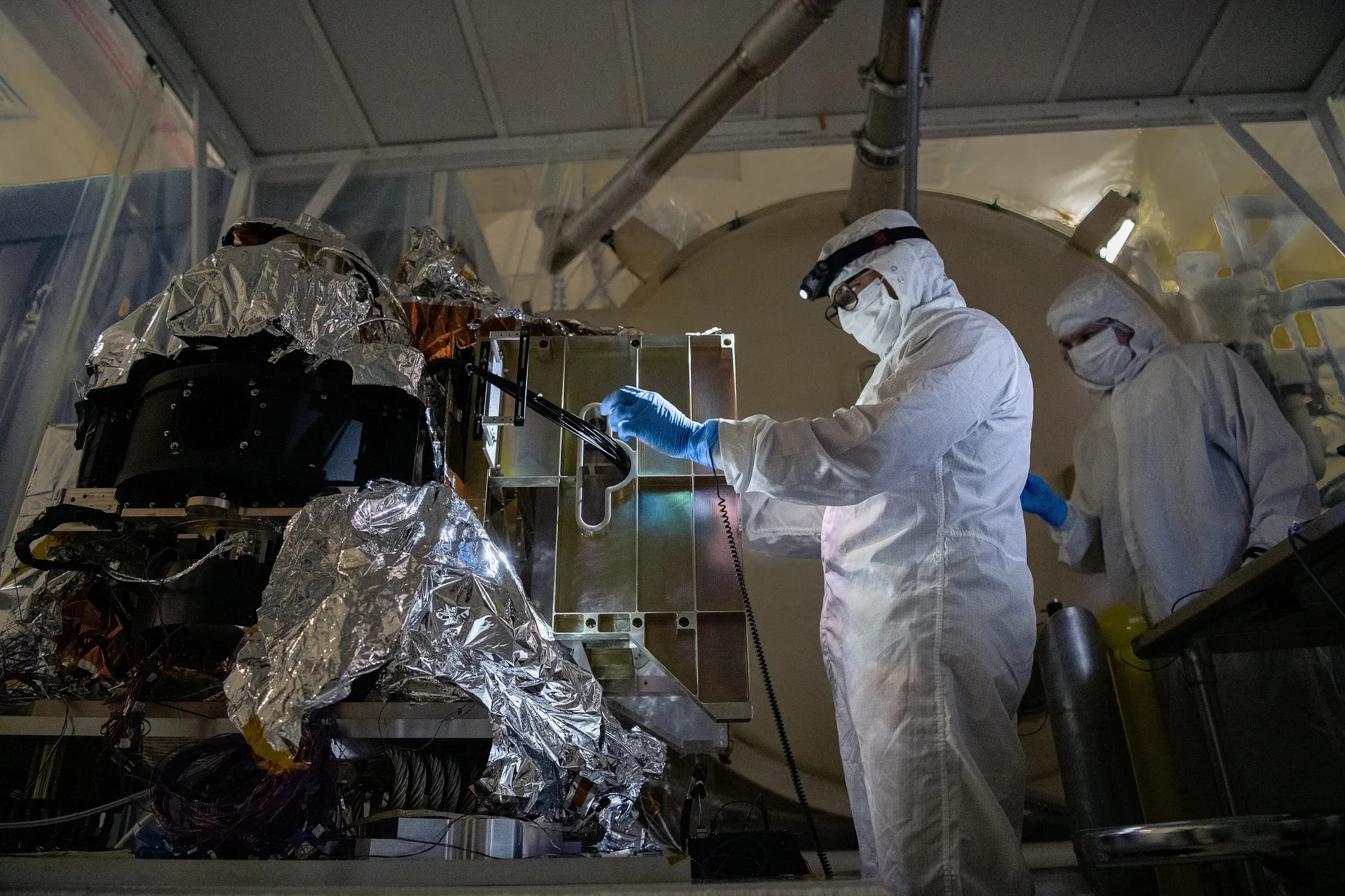
Engineers in cleanroom suits configuring optical fibers on a space instrument.

04 / 06Light

Computers that talk in light.

Single-layer semiconductors emit light efficiently, opening a path to on-chip optics that link tomorrow’s AI clusters at a fraction of the energy.

Photonics team configuring fibers · NASA Goddard
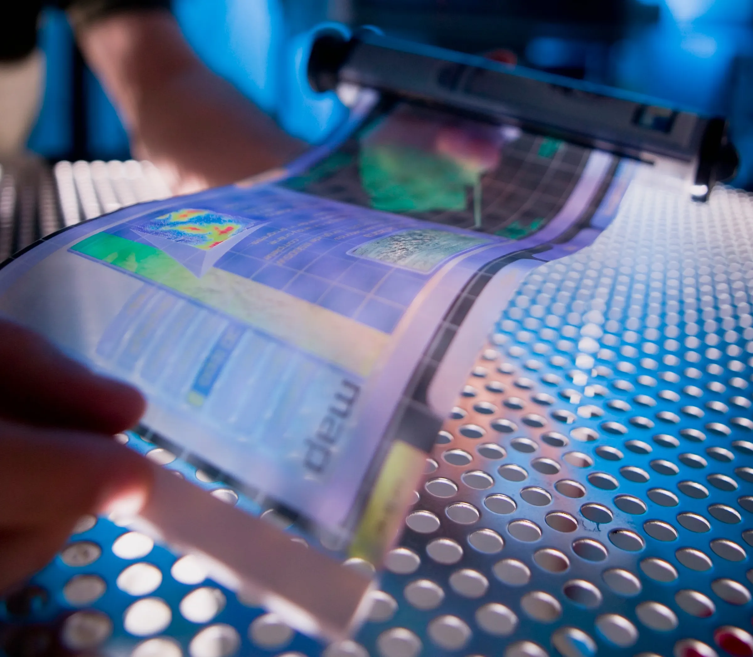
A thin, flexible electronic display being bent by hand.

05 / 06Everywhere

Electronics on anything.

Grown cool enough for glass and plastic, the next materials can bend, flex, and disappear into implants, wearables, and everyday surfaces.4

Flexible display · U.S. Army RDECOM, CC BY 2.0

Northern Europe at night seen from the International Space Station, with city lights below and a green aurora on the horizon.

06 / 06Resilience

Know-how that travels.

Recipes that transfer across tools and sites let advanced manufacturing happen in more places. Critical knowledge stops living inside a handful of companies.

Aurora and city lights from the ISS, Expedition 43 · NASA

  1. Computing, cooled
  2. Space
  3. Medicine
  4. Light
  5. Everywhere
  6. Resilience
MoS₂ · 800 °C · kinetic Monte CarloKMC

The catch

Every one of these is a materials problem.

Each future needs a material controlled at the scale of single atoms, over every square centimeter, run after run. We know what most of these materials are. We can’t yet make them on purpose.

The scale

The next age will be built one atom at a time.

Atoms land, islands nucleate, and a sheet one molecule thick knits itself together. This is a real simulation of monolayer MoS₂, replayed as you scroll.

The stakes

Defects, by design.

At this scale, the same misplaced atom that ruins a device can become a qubit, a light source, or a sensor. The difference is whether you put it there on purpose.

The precedent

Silicon took fifty years to master.

Half a century and trillions of dollars to control one material to parts per billion. The materials that come next can’t wait that long.

Growth simulated atom by atom with Matter42’s kinetic Monte Carlo engine, drawn in the style of an electron micrograph (brightness tracks atomic number). Circled sites are the sulfur vacancies the run produced.

1 nm

Discovery was never the bottleneck.
Making
is.

The missing map 01

Nobody has the map.

Making a material means choosing temperature, pressure, chemistry, substrate, and timing: dozens of coupled knobs. Every lab walks one path through that space by trial and error.

The missing map 02

And every map leaves with its maker.

A lab finds one recipe. It doesn’t transfer to the next tool, and what was learned walks out the door with the person who learned it.

The missing map 03

The same space, mapped.

The recipe the lab settled on was a foothill. The real optimum was somewhere nobody had looked.

Process space · illustrativeillus.10 runs · 10% seen · best recipe 53%
Best recipe foundThe real optimum
↑ Precursor ratioTemperature →

The missing piece

The data to draw the map already exists. Labs pour out spectra, maps, and diffraction every day, then wait days for an expert to read them.
By
the time the answer arrives, the next run has already started blind.

How we’ll make it

We’re mapping how matter is made.

Matter42 connects measurement, physics, and AI into one loop that learns the whole landscape instead of a single point. Where others find a recipe, we find the family.

  1. Measure
  2. Understand
  3. Decide
  4. Make
MeasureUnderstandDecideMakeAtlasone loop
  1. 01Measure

    Read every measurement.

    Atlas reads AFM, Raman, photoluminescence, cathodoluminescence, XRD and more with one engine: tracing islands, finding defects, mapping domains, and pulling out the number that matters.

    Atlas › segment-afm-surface · 82 islands6 techniques · one engine
    • AFMWS₂ islands, MOCVD→0.57 nmmonolayer step · 82 islands traced
    • RamanWS₂, ion-beam patterned→5.5 µmdamage halo found around every milled line
    • CathodoluminescenceInGaN/GaN quantum well, 10 K→1.4×10⁹ cm⁻²nonradiative defects · 85 located
    • XRDGa₂O₃ on Si, annealing series→As grown550 °C700 °C850 °C1000 °Cβ-Ga₂O₃ (400)19 nmβ-Ga₂O₃ crystallites, film crystallizes by 850 °C
    • PhotoluminescenceMoSe₂–WSe₂ lateral heterostructure (CVD)→82 meVWSe₂ shell around a MoSe₂ core, mapped from emission
    • Atlas Physics AIWS₂ defects, simulated vs. measured→measured E₂g widthdefect concentration →5 defect typessimulated, then checked against 553 measured pixels

    Data from five instruments and our physics models, each read by Atlas.

  2. 02Understand

    Ground it in physics.

    Atomistic-to-continuum models predict how a material will behave and explain why, then get checked against what was measured. Here, six simulated defect types meet 553 measured Raman linewidths.

    Atomistic prediction × Raman measurement · WS₂6 defect models · 553 px
    Predicted: E₂g linewidth vs defect concentration (MLIP phonons)
    4812160246810defect concentration, %cm⁻¹measured1.03 %

    Dashed line: median measured linewidth, 7.4 cm⁻¹ after removing instrument broadening and the resonant 2LA(M) band (13.5 → 7.7).

    If every defect were: S→O substitution0.59 % – 1.21 %
    lowhigh

    Every curve states its limits0 K harmonic phonons, MLIP on WS₂ defect supercells, validated against DFT. A linewidth beyond a curve’s computed range is reported as a lower bound, not extrapolated.

    Disagreement is reported, not hiddenAn independent LA(M)/A₁g intensity ratio estimate gives 3.7 ± 1.2 % (calibration transferred from MoS₂; order of magnitude only). Atlas shows both.

  3. 03Decide

    Choose the next run.

    Agents weigh every result against everything learned so far and recommend the next adjustment, so experts spend their time deciding, not deciphering.

    How the work changes with Matter42
    TodayWith Matter42
    Days of manual analysis per resultInterpretation in seconds
    Expert-dependent judgmentPhysics-grounded, repeatable recommendations
    Insight after the runInsight that shapes the next run
    Measurement as overheadMeasurement as the engine
  4. 04Make

    Run it. Learn. Repeat.

    Every run sharpens the map, and every lab on the platform makes the models better for the next one. Our own closed-loop lab pushes the loop further than any single lab could alone.

    60–100×5

    faster iteration than manual, one-knob-at-a-time experimentation.

    Explore Atlas MetrologyExplore Atlas Physics AI

Others discover materials.
We
make them manufacturable.

Why now

Three curves just crossed.

  1. 945 TWh1

    Projected data center demand by 2030

    The world needs new materials.

    Compute, energy, and communications are scaling faster than the materials beneath them. Demand is outrunning the expertise to make what comes next.

  2. 60–100×5

    Faster iteration than manual experimentation

    The models finally work.

    Physics-informed AI now reads spectroscopy and in-situ data the way an expert does, and closes the loop to the next run.

  3. ~100

    Atomically thin semiconductors, most unmapped

    The map is still blank.

    The process know-how for atomic-scale materials is mostly unwritten. Whoever maps it first sets the rules for the next era.

What we believe

  1. 01

    Measurement is the foundation of every breakthrough.

  2. 02

    AI is strongest when it’s grounded in physics, not replacing it.

  3. 03

    Experts should spend their time deciding, not deciphering.

  4. 04

    New materials should reach the world in months, not decades.

The plan

Four steps from the lab bench to the next age.

  1. 1

    Give every materials lab Atlas.

    Every sample, measurement, and recipe, understood in one place.

    Available today: explore Atlas
  2. 2

    Draw the map.

    Connect process to property across thousands of experiments and our own closed-loop lab.

  3. 3

    Make what no one else can.

    Atomically thin materials, and the process know-how that makes them manufacturable.

  4. 4

    Extend to all atomic-scale matter.

    Computing, sensing, photonics, quantum. Every material a few atoms thick, made on purpose.

Atlas is how we learn. The map is what we own.
The
materials are what change the world.

The people

Built by people who’ve measured matter at every scale.

Our founders’ work spans attosecond physics to reactor-scale transport, with more than 500 publications and about 20,000 citations between them. They’re joined by materials scientists, growth experts, and AI researchers, and advised by pioneers in 2D materials.

Meet the team
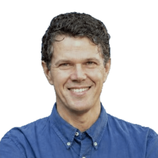
Matthias Kling, PhD

Matthias Kling, PhD

Co-Founder

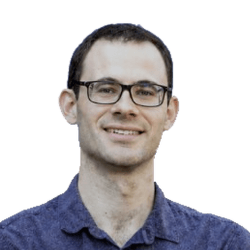
Thomas Linker, PhD

Thomas Linker, PhD

Co-Founder

Kamila Stepniowska

Kamila Stepniowska

Founding Team Member, COO

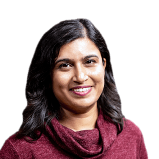
Kalai Ramea, PhD

Kalai Ramea, PhD

Chief AI Officer

Michael Curtis, PhD

Michael Curtis, PhD

Materials Scientist

Srikar Jandhyala, PhD

Srikar Jandhyala, PhD

VP of Product

Bala Radhakrishnan, PhD

Bala Radhakrishnan, PhD

Head of Process Intelligence

Ali Al Kadhim, PhD

Ali Al Kadhim, PhD

Research Engineer

Matt Moderwell

Matt Moderwell

Founding Engineer

Kirtana Romfh

Kirtana Romfh

Multiscale Simulation Engineer

The moonshot

No material should wait a decade to exist.

Every lab and every line measures, understands, and adjusts in real time. New materials go from idea to the world in months. Yield is designed in, not discovered. That’s the world Matter42 is building, with scientists, engineers, partners, and investors who want to make matter do what it has never done.

Talk to the foundersJoin usExplore Atlas

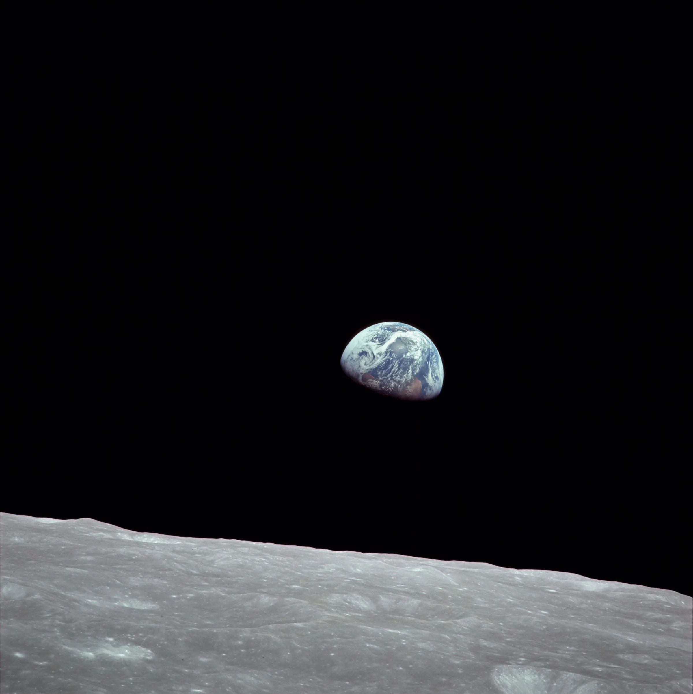
Earthrise, Apollo 8, 1968 · NASA/Bill Anders

Notes

  1. 1.International Energy Agency, Energy and AI (2025): data center electricity demand projected near 945 TWh by 2030.
  2. 2.Roughly two orders of magnitude greater radiation tolerance than silicon; Matter42 whitepaper, “Beyond Moore” (2026).
  3. 3.Spin defects in atomically thin hexagonal boron nitride have been demonstrated as quantum sensors of magnetic field and temperature. Medical applications are a research direction, not a product.
  4. 4.Monolayer growth on polymer and glass substrates near 150 °C has been demonstrated; see Matter42 whitepaper, “Beyond Moore” (2026).
  5. 5.Closed-loop iteration speed versus manual, one-knob-at-a-time experimentation; Matter42 whitepaper, “Beyond Moore” (2026).

Photographs via Wikimedia Commons: NASA, NIMH, and Rsparks3 (public domain / CC0); flexible display by U.S. Army RDECOM, CC BY 2.0. The growth run is a kinetic Monte Carlo simulation; the process landscape is illustrative. Every other figure is measured data.

Matter42

A world model for your materials: know what you made and decide what to make next, with the evidence attached.

Platform

  • Atlas Metrology
  • Atlas Physics AI
  • Literature

Software

  • Raman analysis
  • PL analysis
  • XPS analysis
  • XRD analysis
  • AFM analysis

Company

  • Vision
  • Team
  • Careers
  • Blog

Resources

  • Documentation
  • Python SDK
  • Security and deployment
  • FAQ

Legal

  • Privacy Policy
  • Terms and Conditions

Social

  • LinkedIn

Copyright © 2026 Matter42. All rights reserved.

Matter42
  • Vision
Sign in

Matter42 Atlas

  • Atlas Metrology
  • Atlas Physics AI

Resources

  • Security
  • FAQ
  • Documentation
  • Python SDK

Company

  • Team
  • Careers
  • Blog
Vision
Sign in

The Matter42 vision

Everything we want next is made of something we can’t make yet.

Cooler computers. Sensors that read a single cell. Electronics that survive deep space, speak in light, and bend like paper. Every one of them is waiting on a material.

See what becomes possibleHow we’ll make it

What becomes possible

Rows of cooling fans on the roof of a data center.

01 / 06Computing, cooled

Intelligence without the heat.

Devices that switch with a fraction of today’s energy mean data centers that draw less power, shed less heat, and drink less water. AI keeps scaling; the grid doesn’t break.1

Data center cooling · Rsparks3, CC0

The Hubble Space Telescope drifting in black space after release from Space Shuttle Atlantis.

02 / 06Space

Electronics built for the dark.

A material a few atoms thick gives radiation almost nothing to hit. Lighter satellites, longer missions, and compute in orbit and beyond.2

Hubble after release from Atlantis, 2009 · NASA

A person seated in a magnetoencephalography scanner that records the brain’s magnetic fields.

03 / 06Medicine

Sensors that see a single cell.

Place one defect on purpose and a crystal becomes a quantum sensor. Only atoms thick, it can sit nanometers from living tissue: toward brain imaging without cryogenics, and magnetic resonance at the scale of a molecule.3

Magnetoencephalography scanner · NIMH

Engineers in cleanroom suits configuring optical fibers on a space instrument.

04 / 06Light

Computers that talk in light.

Single-layer semiconductors emit light efficiently, opening a path to on-chip optics that link tomorrow’s AI clusters at a fraction of the energy.

Photonics team configuring fibers · NASA Goddard

A thin, flexible electronic display being bent by hand.

05 / 06Everywhere

Electronics on anything.

Grown cool enough for glass and plastic, the next materials can bend, flex, and disappear into implants, wearables, and everyday surfaces.4

Flexible display · U.S. Army RDECOM, CC BY 2.0

Northern Europe at night seen from the International Space Station, with city lights below and a green aurora on the horizon.

06 / 06Resilience

Know-how that travels.

Recipes that transfer across tools and sites let advanced manufacturing happen in more places. Critical knowledge stops living inside a handful of companies.

Aurora and city lights from the ISS, Expedition 43 · NASA

  1. Computing, cooled
  2. Space
  3. Medicine
  4. Light
  5. Everywhere
  6. Resilience
MoS₂ · 800 °C · kinetic Monte CarloKMC

The catch

Every one of these is a materials problem.

Each future needs a material controlled at the scale of single atoms, over every square centimeter, run after run. We know what most of these materials are. We can’t yet make them on purpose.

The scale

The next age will be built one atom at a time.

Atoms land, islands nucleate, and a sheet one molecule thick knits itself together. This is a real simulation of monolayer MoS₂, replayed as you scroll.

The stakes

Defects, by design.

At this scale, the same misplaced atom that ruins a device can become a qubit, a light source, or a sensor. The difference is whether you put it there on purpose.

The precedent

Silicon took fifty years to master.

Half a century and trillions of dollars to control one material to parts per billion. The materials that come next can’t wait that long.

Growth simulated atom by atom with Matter42’s kinetic Monte Carlo engine, drawn in the style of an electron micrograph (brightness tracks atomic number). Circled sites are the sulfur vacancies the run produced.

1 nm

Discovery was never the bottleneck.
Making
is.

The missing map 01

Nobody has the map.

Making a material means choosing temperature, pressure, chemistry, substrate, and timing: dozens of coupled knobs. Every lab walks one path through that space by trial and error.

The missing map 02

And every map leaves with its maker.

A lab finds one recipe. It doesn’t transfer to the next tool, and what was learned walks out the door with the person who learned it.

The missing map 03

The same space, mapped.

The recipe the lab settled on was a foothill. The real optimum was somewhere nobody had looked.

Process space · illustrativeillus.10 runs · 10% seen · best recipe 53%
Best recipe foundThe real optimum
↑ Precursor ratioTemperature →

The missing piece

The data to draw the map already exists. Labs pour out spectra, maps, and diffraction every day, then wait days for an expert to read them.
By
the time the answer arrives, the next run has already started blind.

How we’ll make it

We’re mapping how matter is made.

Matter42 connects measurement, physics, and AI into one loop that learns the whole landscape instead of a single point. Where others find a recipe, we find the family.

  1. Measure
  2. Understand
  3. Decide
  4. Make
MeasureUnderstandDecideMakeAtlasone loop
  1. 01Measure

    Read every measurement.

    Atlas reads AFM, Raman, photoluminescence, cathodoluminescence, XRD and more with one engine: tracing islands, finding defects, mapping domains, and pulling out the number that matters.

    Atlas › segment-afm-surface · 82 islands6 techniques · one engine
    • AFMWS₂ islands, MOCVD→0.57 nmmonolayer step · 82 islands traced
    • RamanWS₂, ion-beam patterned→5.5 µmdamage halo found around every milled line
    • CathodoluminescenceInGaN/GaN quantum well, 10 K→1.4×10⁹ cm⁻²nonradiative defects · 85 located
    • XRDGa₂O₃ on Si, annealing series→As grown550 °C700 °C850 °C1000 °Cβ-Ga₂O₃ (400)19 nmβ-Ga₂O₃ crystallites, film crystallizes by 850 °C
    • PhotoluminescenceMoSe₂–WSe₂ lateral heterostructure (CVD)→82 meVWSe₂ shell around a MoSe₂ core, mapped from emission
    • Atlas Physics AIWS₂ defects, simulated vs. measured→measured E₂g widthdefect concentration →5 defect typessimulated, then checked against 553 measured pixels

    Data from five instruments and our physics models, each read by Atlas.

  2. 02Understand

    Ground it in physics.

    Atomistic-to-continuum models predict how a material will behave and explain why, then get checked against what was measured. Here, six simulated defect types meet 553 measured Raman linewidths.

    Atomistic prediction × Raman measurement · WS₂6 defect models · 553 px
    Predicted: E₂g linewidth vs defect concentration (MLIP phonons)
    4812160246810defect concentration, %cm⁻¹measured1.03 %

    Dashed line: median measured linewidth, 7.4 cm⁻¹ after removing instrument broadening and the resonant 2LA(M) band (13.5 → 7.7).

    If every defect were: S→O substitution0.59 % – 1.21 %
    lowhigh

    Every curve states its limits0 K harmonic phonons, MLIP on WS₂ defect supercells, validated against DFT. A linewidth beyond a curve’s computed range is reported as a lower bound, not extrapolated.

    Disagreement is reported, not hiddenAn independent LA(M)/A₁g intensity ratio estimate gives 3.7 ± 1.2 % (calibration transferred from MoS₂; order of magnitude only). Atlas shows both.

  3. 03Decide

    Choose the next run.

    Agents weigh every result against everything learned so far and recommend the next adjustment, so experts spend their time deciding, not deciphering.

    How the work changes with Matter42
    TodayWith Matter42
    Days of manual analysis per resultInterpretation in seconds
    Expert-dependent judgmentPhysics-grounded, repeatable recommendations
    Insight after the runInsight that shapes the next run
    Measurement as overheadMeasurement as the engine
  4. 04Make

    Run it. Learn. Repeat.

    Every run sharpens the map, and every lab on the platform makes the models better for the next one. Our own closed-loop lab pushes the loop further than any single lab could alone.

    60–100×5

    faster iteration than manual, one-knob-at-a-time experimentation.

    Explore Atlas MetrologyExplore Atlas Physics AI

Others discover materials.
We
make them manufacturable.

Why now

Three curves just crossed.

  1. 945 TWh1

    Projected data center demand by 2030

    The world needs new materials.

    Compute, energy, and communications are scaling faster than the materials beneath them. Demand is outrunning the expertise to make what comes next.

  2. 60–100×5

    Faster iteration than manual experimentation

    The models finally work.

    Physics-informed AI now reads spectroscopy and in-situ data the way an expert does, and closes the loop to the next run.

  3. ~100

    Atomically thin semiconductors, most unmapped

    The map is still blank.

    The process know-how for atomic-scale materials is mostly unwritten. Whoever maps it first sets the rules for the next era.

What we believe

  1. 01

    Measurement is the foundation of every breakthrough.

  2. 02

    AI is strongest when it’s grounded in physics, not replacing it.

  3. 03

    Experts should spend their time deciding, not deciphering.

  4. 04

    New materials should reach the world in months, not decades.

The plan

Four steps from the lab bench to the next age.

  1. 1

    Give every materials lab Atlas.

    Every sample, measurement, and recipe, understood in one place.

    Available today: explore Atlas
  2. 2

    Draw the map.

    Connect process to property across thousands of experiments and our own closed-loop lab.

  3. 3

    Make what no one else can.

    Atomically thin materials, and the process know-how that makes them manufacturable.

  4. 4

    Extend to all atomic-scale matter.

    Computing, sensing, photonics, quantum. Every material a few atoms thick, made on purpose.

Atlas is how we learn. The map is what we own.
The
materials are what change the world.

The people

Built by people who’ve measured matter at every scale.

Our founders’ work spans attosecond physics to reactor-scale transport, with more than 500 publications and about 20,000 citations between them. They’re joined by materials scientists, growth experts, and AI researchers, and advised by pioneers in 2D materials.

Meet the team

Matthias Kling, PhD

Matthias Kling, PhD

Co-Founder

Thomas Linker, PhD

Thomas Linker, PhD

Co-Founder

Kamila Stepniowska

Kamila Stepniowska

Founding Team Member, COO

Kalai Ramea, PhD

Kalai Ramea, PhD

Chief AI Officer

Michael Curtis, PhD

Michael Curtis, PhD

Materials Scientist

Srikar Jandhyala, PhD

Srikar Jandhyala, PhD

VP of Product

Bala Radhakrishnan, PhD

Bala Radhakrishnan, PhD

Head of Process Intelligence

Ali Al Kadhim, PhD

Ali Al Kadhim, PhD

Research Engineer

Matt Moderwell

Matt Moderwell

Founding Engineer

Kirtana Romfh

Kirtana Romfh

Multiscale Simulation Engineer

The moonshot

No material should wait a decade to exist.

Every lab and every line measures, understands, and adjusts in real time. New materials go from idea to the world in months. Yield is designed in, not discovered. That’s the world Matter42 is building, with scientists, engineers, partners, and investors who want to make matter do what it has never done.

Talk to the foundersJoin usExplore Atlas

Earthrise, Apollo 8, 1968 · NASA/Bill Anders

Notes

  1. 1.International Energy Agency, Energy and AI (2025): data center electricity demand projected near 945 TWh by 2030.
  2. 2.Roughly two orders of magnitude greater radiation tolerance than silicon; Matter42 whitepaper, “Beyond Moore” (2026).
  3. 3.Spin defects in atomically thin hexagonal boron nitride have been demonstrated as quantum sensors of magnetic field and temperature. Medical applications are a research direction, not a product.
  4. 4.Monolayer growth on polymer and glass substrates near 150 °C has been demonstrated; see Matter42 whitepaper, “Beyond Moore” (2026).
  5. 5.Closed-loop iteration speed versus manual, one-knob-at-a-time experimentation; Matter42 whitepaper, “Beyond Moore” (2026).

Photographs via Wikimedia Commons: NASA, NIMH, and Rsparks3 (public domain / CC0); flexible display by U.S. Army RDECOM, CC BY 2.0. The growth run is a kinetic Monte Carlo simulation; the process landscape is illustrative. Every other figure is measured data.

Matter42

A world model for your materials: know what you made and decide what to make next, with the evidence attached.

Platform

  • Atlas Metrology
  • Atlas Physics AI
  • Literature

Software

  • Raman analysis
  • PL analysis
  • XPS analysis
  • XRD analysis
  • AFM analysis

Company

  • Vision
  • Team
  • Careers
  • Blog

Resources

  • Documentation
  • Python SDK
  • Security and deployment
  • FAQ

Legal

  • Privacy Policy
  • Terms and Conditions

Social

  • LinkedIn

Copyright © 2026 Matter42. All rights reserved.

Matter42
  • Vision
Sign in

Matter42 Atlas

  • Atlas Metrology
  • Atlas Physics AI

Resources

  • Security
  • FAQ
  • Documentation
  • Python SDK

Company

  • Team
  • Careers
  • Blog
Vision
Sign in

The Matter42 vision

Everything we want next is made of something we can’t make yet.

Cooler computers. Sensors that read a single cell. Electronics that survive deep space, speak in light, and bend like paper. Every one of them is waiting on a material.

See what becomes possibleHow we’ll make it

What becomes possible

Rows of cooling fans on the roof of a data center.

01 / 06Computing, cooled

Intelligence without the heat.

Devices that switch with a fraction of today’s energy mean data centers that draw less power, shed less heat, and drink less water. AI keeps scaling; the grid doesn’t break.1

Data center cooling · Rsparks3, CC0

The Hubble Space Telescope drifting in black space after release from Space Shuttle Atlantis.

02 / 06Space

Electronics built for the dark.

A material a few atoms thick gives radiation almost nothing to hit. Lighter satellites, longer missions, and compute in orbit and beyond.2

Hubble after release from Atlantis, 2009 · NASA

A person seated in a magnetoencephalography scanner that records the brain’s magnetic fields.

03 / 06Medicine

Sensors that see a single cell.

Place one defect on purpose and a crystal becomes a quantum sensor. Only atoms thick, it can sit nanometers from living tissue: toward brain imaging without cryogenics, and magnetic resonance at the scale of a molecule.3

Magnetoencephalography scanner · NIMH

Engineers in cleanroom suits configuring optical fibers on a space instrument.

04 / 06Light

Computers that talk in light.

Single-layer semiconductors emit light efficiently, opening a path to on-chip optics that link tomorrow’s AI clusters at a fraction of the energy.

Photonics team configuring fibers · NASA Goddard

A thin, flexible electronic display being bent by hand.

05 / 06Everywhere

Electronics on anything.

Grown cool enough for glass and plastic, the next materials can bend, flex, and disappear into implants, wearables, and everyday surfaces.4

Flexible display · U.S. Army RDECOM, CC BY 2.0

Northern Europe at night seen from the International Space Station, with city lights below and a green aurora on the horizon.

06 / 06Resilience

Know-how that travels.

Recipes that transfer across tools and sites let advanced manufacturing happen in more places. Critical knowledge stops living inside a handful of companies.

Aurora and city lights from the ISS, Expedition 43 · NASA

  1. Computing, cooled
  2. Space
  3. Medicine
  4. Light
  5. Everywhere
  6. Resilience
MoS₂ · 800 °C · kinetic Monte CarloKMC

The catch

Every one of these is a materials problem.

Each future needs a material controlled at the scale of single atoms, over every square centimeter, run after run. We know what most of these materials are. We can’t yet make them on purpose.

The scale

The next age will be built one atom at a time.

Atoms land, islands nucleate, and a sheet one molecule thick knits itself together. This is a real simulation of monolayer MoS₂, replayed as you scroll.

The stakes

Defects, by design.

At this scale, the same misplaced atom that ruins a device can become a qubit, a light source, or a sensor. The difference is whether you put it there on purpose.

The precedent

Silicon took fifty years to master.

Half a century and trillions of dollars to control one material to parts per billion. The materials that come next can’t wait that long.

Growth simulated atom by atom with Matter42’s kinetic Monte Carlo engine, drawn in the style of an electron micrograph (brightness tracks atomic number). Circled sites are the sulfur vacancies the run produced.

1 nm

Discovery was never the bottleneck.
Making
is.

The missing map 01

Nobody has the map.

Making a material means choosing temperature, pressure, chemistry, substrate, and timing: dozens of coupled knobs. Every lab walks one path through that space by trial and error.

The missing map 02

And every map leaves with its maker.

A lab finds one recipe. It doesn’t transfer to the next tool, and what was learned walks out the door with the person who learned it.

The missing map 03

The same space, mapped.

The recipe the lab settled on was a foothill. The real optimum was somewhere nobody had looked.

Process space · illustrativeillus.10 runs · 10% seen · best recipe 53%
Best recipe foundThe real optimum
↑ Precursor ratioTemperature →

The missing piece

The data to draw the map already exists. Labs pour out spectra, maps, and diffraction every day, then wait days for an expert to read them.
By
the time the answer arrives, the next run has already started blind.

How we’ll make it

We’re mapping how matter is made.

Matter42 connects measurement, physics, and AI into one loop that learns the whole landscape instead of a single point. Where others find a recipe, we find the family.

  1. Measure
  2. Understand
  3. Decide
  4. Make
MeasureUnderstandDecideMakeAtlasone loop
  1. 01Measure

    Read every measurement.

    Atlas reads AFM, Raman, photoluminescence, cathodoluminescence, XRD and more with one engine: tracing islands, finding defects, mapping domains, and pulling out the number that matters.

    Atlas › segment-afm-surface · 82 islands6 techniques · one engine
    • AFMWS₂ islands, MOCVD→0.57 nmmonolayer step · 82 islands traced
    • RamanWS₂, ion-beam patterned→5.5 µmdamage halo found around every milled line
    • CathodoluminescenceInGaN/GaN quantum well, 10 K→1.4×10⁹ cm⁻²nonradiative defects · 85 located
    • XRDGa₂O₃ on Si, annealing series→As grown550 °C700 °C850 °C1000 °Cβ-Ga₂O₃ (400)19 nmβ-Ga₂O₃ crystallites, film crystallizes by 850 °C
    • PhotoluminescenceMoSe₂–WSe₂ lateral heterostructure (CVD)→82 meVWSe₂ shell around a MoSe₂ core, mapped from emission
    • Atlas Physics AIWS₂ defects, simulated vs. measured→measured E₂g widthdefect concentration →5 defect typessimulated, then checked against 553 measured pixels

    Data from five instruments and our physics models, each read by Atlas.

  2. 02Understand

    Ground it in physics.

    Atomistic-to-continuum models predict how a material will behave and explain why, then get checked against what was measured. Here, six simulated defect types meet 553 measured Raman linewidths.

    Atomistic prediction × Raman measurement · WS₂6 defect models · 553 px
    Predicted: E₂g linewidth vs defect concentration (MLIP phonons)
    4812160246810defect concentration, %cm⁻¹measured1.03 %

    Dashed line: median measured linewidth, 7.4 cm⁻¹ after removing instrument broadening and the resonant 2LA(M) band (13.5 → 7.7).

    If every defect were: S→O substitution0.59 % – 1.21 %
    lowhigh

    Every curve states its limits0 K harmonic phonons, MLIP on WS₂ defect supercells, validated against DFT. A linewidth beyond a curve’s computed range is reported as a lower bound, not extrapolated.

    Disagreement is reported, not hiddenAn independent LA(M)/A₁g intensity ratio estimate gives 3.7 ± 1.2 % (calibration transferred from MoS₂; order of magnitude only). Atlas shows both.

  3. 03Decide

    Choose the next run.

    Agents weigh every result against everything learned so far and recommend the next adjustment, so experts spend their time deciding, not deciphering.

    How the work changes with Matter42
    TodayWith Matter42
    Days of manual analysis per resultInterpretation in seconds
    Expert-dependent judgmentPhysics-grounded, repeatable recommendations
    Insight after the runInsight that shapes the next run
    Measurement as overheadMeasurement as the engine
  4. 04Make

    Run it. Learn. Repeat.

    Every run sharpens the map, and every lab on the platform makes the models better for the next one. Our own closed-loop lab pushes the loop further than any single lab could alone.

    60–100×5

    faster iteration than manual, one-knob-at-a-time experimentation.

    Explore Atlas MetrologyExplore Atlas Physics AI

Others discover materials.
We
make them manufacturable.

Why now

Three curves just crossed.

  1. 945 TWh1

    Projected data center demand by 2030

    The world needs new materials.

    Compute, energy, and communications are scaling faster than the materials beneath them. Demand is outrunning the expertise to make what comes next.

  2. 60–100×5

    Faster iteration than manual experimentation

    The models finally work.

    Physics-informed AI now reads spectroscopy and in-situ data the way an expert does, and closes the loop to the next run.

  3. ~100

    Atomically thin semiconductors, most unmapped

    The map is still blank.

    The process know-how for atomic-scale materials is mostly unwritten. Whoever maps it first sets the rules for the next era.

What we believe

  1. 01

    Measurement is the foundation of every breakthrough.

  2. 02

    AI is strongest when it’s grounded in physics, not replacing it.

  3. 03

    Experts should spend their time deciding, not deciphering.

  4. 04

    New materials should reach the world in months, not decades.

The plan

Four steps from the lab bench to the next age.

  1. 1

    Give every materials lab Atlas.

    Every sample, measurement, and recipe, understood in one place.

    Available today: explore Atlas
  2. 2

    Draw the map.

    Connect process to property across thousands of experiments and our own closed-loop lab.

  3. 3

    Make what no one else can.

    Atomically thin materials, and the process know-how that makes them manufacturable.

  4. 4

    Extend to all atomic-scale matter.

    Computing, sensing, photonics, quantum. Every material a few atoms thick, made on purpose.

Atlas is how we learn. The map is what we own.
The
materials are what change the world.

The people

Built by people who’ve measured matter at every scale.

Our founders’ work spans attosecond physics to reactor-scale transport, with more than 500 publications and about 20,000 citations between them. They’re joined by materials scientists, growth experts, and AI researchers, and advised by pioneers in 2D materials.

Meet the team
Matthias Kling, PhD

Matthias Kling, PhD

Co-Founder

Thomas Linker, PhD

Thomas Linker, PhD

Co-Founder

Kamila Stepniowska

Kamila Stepniowska

Founding Team Member, COO

Kalai Ramea, PhD

Kalai Ramea, PhD

Chief AI Officer

Michael Curtis, PhD

Michael Curtis, PhD

Materials Scientist

Srikar Jandhyala, PhD

Srikar Jandhyala, PhD

VP of Product

Bala Radhakrishnan, PhD

Bala Radhakrishnan, PhD

Head of Process Intelligence

Ali Al Kadhim, PhD

Ali Al Kadhim, PhD

Research Engineer

Matt Moderwell

Matt Moderwell

Founding Engineer

Kirtana Romfh

Kirtana Romfh

Multiscale Simulation Engineer

The moonshot

No material should wait a decade to exist.

Every lab and every line measures, understands, and adjusts in real time. New materials go from idea to the world in months. Yield is designed in, not discovered. That’s the world Matter42 is building, with scientists, engineers, partners, and investors who want to make matter do what it has never done.

Talk to the foundersJoin usExplore Atlas

Earthrise, Apollo 8, 1968 · NASA/Bill Anders

Notes

  1. 1.International Energy Agency, Energy and AI (2025): data center electricity demand projected near 945 TWh by 2030.
  2. 2.Roughly two orders of magnitude greater radiation tolerance than silicon; Matter42 whitepaper, “Beyond Moore” (2026).
  3. 3.Spin defects in atomically thin hexagonal boron nitride have been demonstrated as quantum sensors of magnetic field and temperature. Medical applications are a research direction, not a product.
  4. 4.Monolayer growth on polymer and glass substrates near 150 °C has been demonstrated; see Matter42 whitepaper, “Beyond Moore” (2026).
  5. 5.Closed-loop iteration speed versus manual, one-knob-at-a-time experimentation; Matter42 whitepaper, “Beyond Moore” (2026).

Photographs via Wikimedia Commons: NASA, NIMH, and Rsparks3 (public domain / CC0); flexible display by U.S. Army RDECOM, CC BY 2.0. The growth run is a kinetic Monte Carlo simulation; the process landscape is illustrative. Every other figure is measured data.

Matter42

A world model for your materials: know what you made and decide what to make next, with the evidence attached.

Platform

  • Atlas Metrology
  • Atlas Physics AI
  • Literature

Software

  • Raman analysis
  • PL analysis
  • XPS analysis
  • XRD analysis
  • AFM analysis

Company

  • Vision
  • Team
  • Careers
  • Blog

Resources

  • Documentation
  • Python SDK
  • Security and deployment
  • FAQ

Legal

  • Privacy Policy
  • Terms and Conditions

Social

  • LinkedIn

Copyright © 2026 Matter42. All rights reserved.

Matter42
  • Vision
Sign in

Matter42 Atlas

  • Atlas Metrology
  • Atlas Physics AI

Resources

  • Security
  • FAQ
  • Documentation
  • Python SDK

Company

  • Team
  • Careers
  • Blog
Vision
Sign in

The Matter42 vision

Everything we want next is made of something we can’t make yet.

Cooler computers. Sensors that read a single cell. Electronics that survive deep space, speak in light, and bend like paper. Every one of them is waiting on a material.

See what becomes possibleHow we’ll make it

What becomes possible

Rows of cooling fans on the roof of a data center.

01 / 06Computing, cooled

Intelligence without the heat.

Devices that switch with a fraction of today’s energy mean data centers that draw less power, shed less heat, and drink less water. AI keeps scaling; the grid doesn’t break.1

Data center cooling · Rsparks3, CC0

The Hubble Space Telescope drifting in black space after release from Space Shuttle Atlantis.

02 / 06Space

Electronics built for the dark.

A material a few atoms thick gives radiation almost nothing to hit. Lighter satellites, longer missions, and compute in orbit and beyond.2

Hubble after release from Atlantis, 2009 · NASA

A person seated in a magnetoencephalography scanner that records the brain’s magnetic fields.

03 / 06Medicine

Sensors that see a single cell.

Place one defect on purpose and a crystal becomes a quantum sensor. Only atoms thick, it can sit nanometers from living tissue: toward brain imaging without cryogenics, and magnetic resonance at the scale of a molecule.3

Magnetoencephalography scanner · NIMH

Engineers in cleanroom suits configuring optical fibers on a space instrument.

04 / 06Light

Computers that talk in light.

Single-layer semiconductors emit light efficiently, opening a path to on-chip optics that link tomorrow’s AI clusters at a fraction of the energy.

Photonics team configuring fibers · NASA Goddard

A thin, flexible electronic display being bent by hand.

05 / 06Everywhere

Electronics on anything.

Grown cool enough for glass and plastic, the next materials can bend, flex, and disappear into implants, wearables, and everyday surfaces.4

Flexible display · U.S. Army RDECOM, CC BY 2.0

Northern Europe at night seen from the International Space Station, with city lights below and a green aurora on the horizon.

06 / 06Resilience

Know-how that travels.

Recipes that transfer across tools and sites let advanced manufacturing happen in more places. Critical knowledge stops living inside a handful of companies.

Aurora and city lights from the ISS, Expedition 43 · NASA

  1. Computing, cooled
  2. Space
  3. Medicine
  4. Light
  5. Everywhere
  6. Resilience
MoS₂ · 800 °C · kinetic Monte CarloKMC

The catch

Every one of these is a materials problem.

Each future needs a material controlled at the scale of single atoms, over every square centimeter, run after run. We know what most of these materials are. We can’t yet make them on purpose.

The scale

The next age will be built one atom at a time.

Atoms land, islands nucleate, and a sheet one molecule thick knits itself together. This is a real simulation of monolayer MoS₂, replayed as you scroll.

The stakes

Defects, by design.

At this scale, the same misplaced atom that ruins a device can become a qubit, a light source, or a sensor. The difference is whether you put it there on purpose.

The precedent

Silicon took fifty years to master.

Half a century and trillions of dollars to control one material to parts per billion. The materials that come next can’t wait that long.

Growth simulated atom by atom with Matter42’s kinetic Monte Carlo engine, drawn in the style of an electron micrograph (brightness tracks atomic number). Circled sites are the sulfur vacancies the run produced.

1 nm

Discovery was never the bottleneck.
Making
is.

The missing map 01

Nobody has the map.

Making a material means choosing temperature, pressure, chemistry, substrate, and timing: dozens of coupled knobs. Every lab walks one path through that space by trial and error.

The missing map 02

And every map leaves with its maker.

A lab finds one recipe. It doesn’t transfer to the next tool, and what was learned walks out the door with the person who learned it.

The missing map 03

The same space, mapped.

The recipe the lab settled on was a foothill. The real optimum was somewhere nobody had looked.

Process space · illustrativeillus.10 runs · 10% seen · best recipe 53%
Best recipe foundThe real optimum
↑ Precursor ratioTemperature →

The missing piece

The data to draw the map already exists. Labs pour out spectra, maps, and diffraction every day, then wait days for an expert to read them.
By
the time the answer arrives, the next run has already started blind.

How we’ll make it

We’re mapping how matter is made.

Matter42 connects measurement, physics, and AI into one loop that learns the whole landscape instead of a single point. Where others find a recipe, we find the family.

  1. Measure
  2. Understand
  3. Decide
  4. Make
MeasureUnderstandDecideMakeAtlasone loop
  1. 01Measure

    Read every measurement.

    Atlas reads AFM, Raman, photoluminescence, cathodoluminescence, XRD and more with one engine: tracing islands, finding defects, mapping domains, and pulling out the number that matters.

    Atlas › segment-afm-surface · 82 islands6 techniques · one engine
    • AFMWS₂ islands, MOCVD→0.57 nmmonolayer step · 82 islands traced
    • RamanWS₂, ion-beam patterned→5.5 µmdamage halo found around every milled line
    • CathodoluminescenceInGaN/GaN quantum well, 10 K→1.4×10⁹ cm⁻²nonradiative defects · 85 located
    • XRDGa₂O₃ on Si, annealing series→As grown550 °C700 °C850 °C1000 °Cβ-Ga₂O₃ (400)19 nmβ-Ga₂O₃ crystallites, film crystallizes by 850 °C
    • PhotoluminescenceMoSe₂–WSe₂ lateral heterostructure (CVD)→82 meVWSe₂ shell around a MoSe₂ core, mapped from emission
    • Atlas Physics AIWS₂ defects, simulated vs. measured→measured E₂g widthdefect concentration →5 defect typessimulated, then checked against 553 measured pixels

    Data from five instruments and our physics models, each read by Atlas.

  2. 02Understand

    Ground it in physics.

    Atomistic-to-continuum models predict how a material will behave and explain why, then get checked against what was measured. Here, six simulated defect types meet 553 measured Raman linewidths.

    Atomistic prediction × Raman measurement · WS₂6 defect models · 553 px
    Predicted: E₂g linewidth vs defect concentration (MLIP phonons)
    4812160246810defect concentration, %cm⁻¹measured1.03 %

    Dashed line: median measured linewidth, 7.4 cm⁻¹ after removing instrument broadening and the resonant 2LA(M) band (13.5 → 7.7).

    If every defect were: S→O substitution0.59 % – 1.21 %
    lowhigh

    Every curve states its limits0 K harmonic phonons, MLIP on WS₂ defect supercells, validated against DFT. A linewidth beyond a curve’s computed range is reported as a lower bound, not extrapolated.

    Disagreement is reported, not hiddenAn independent LA(M)/A₁g intensity ratio estimate gives 3.7 ± 1.2 % (calibration transferred from MoS₂; order of magnitude only). Atlas shows both.

  3. 03Decide

    Choose the next run.

    Agents weigh every result against everything learned so far and recommend the next adjustment, so experts spend their time deciding, not deciphering.

    How the work changes with Matter42
    TodayWith Matter42
    Days of manual analysis per resultInterpretation in seconds
    Expert-dependent judgmentPhysics-grounded, repeatable recommendations
    Insight after the runInsight that shapes the next run
    Measurement as overheadMeasurement as the engine
  4. 04Make

    Run it. Learn. Repeat.

    Every run sharpens the map, and every lab on the platform makes the models better for the next one. Our own closed-loop lab pushes the loop further than any single lab could alone.

    60–100×5

    faster iteration than manual, one-knob-at-a-time experimentation.

    Explore Atlas MetrologyExplore Atlas Physics AI

Others discover materials.
We
make them manufacturable.

Why now

Three curves just crossed.

  1. 945 TWh1

    Projected data center demand by 2030

    The world needs new materials.

    Compute, energy, and communications are scaling faster than the materials beneath them. Demand is outrunning the expertise to make what comes next.

  2. 60–100×5

    Faster iteration than manual experimentation

    The models finally work.

    Physics-informed AI now reads spectroscopy and in-situ data the way an expert does, and closes the loop to the next run.

  3. ~100

    Atomically thin semiconductors, most unmapped

    The map is still blank.

    The process know-how for atomic-scale materials is mostly unwritten. Whoever maps it first sets the rules for the next era.

What we believe

  1. 01

    Measurement is the foundation of every breakthrough.

  2. 02

    AI is strongest when it’s grounded in physics, not replacing it.

  3. 03

    Experts should spend their time deciding, not deciphering.

  4. 04

    New materials should reach the world in months, not decades.

The plan

Four steps from the lab bench to the next age.

  1. 1

    Give every materials lab Atlas.

    Every sample, measurement, and recipe, understood in one place.

    Available today: explore Atlas
  2. 2

    Draw the map.

    Connect process to property across thousands of experiments and our own closed-loop lab.

  3. 3

    Make what no one else can.

    Atomically thin materials, and the process know-how that makes them manufacturable.

  4. 4

    Extend to all atomic-scale matter.

    Computing, sensing, photonics, quantum. Every material a few atoms thick, made on purpose.

Atlas is how we learn. The map is what we own.
The
materials are what change the world.

The people

Built by people who’ve measured matter at every scale.

Our founders’ work spans attosecond physics to reactor-scale transport, with more than 500 publications and about 20,000 citations between them. They’re joined by materials scientists, growth experts, and AI researchers, and advised by pioneers in 2D materials.

Meet the team
Matthias Kling, PhD

Matthias Kling, PhD

Co-Founder

Thomas Linker, PhD

Thomas Linker, PhD

Co-Founder

Kamila Stepniowska

Kamila Stepniowska

Founding Team Member, COO

Kalai Ramea, PhD

Kalai Ramea, PhD

Chief AI Officer

Michael Curtis, PhD

Michael Curtis, PhD

Materials Scientist

Srikar Jandhyala, PhD

Srikar Jandhyala, PhD

VP of Product

Bala Radhakrishnan, PhD

Bala Radhakrishnan, PhD

Head of Process Intelligence

Ali Al Kadhim, PhD

Ali Al Kadhim, PhD

Research Engineer

Matt Moderwell

Matt Moderwell

Founding Engineer

Kirtana Romfh

Kirtana Romfh

Multiscale Simulation Engineer

The moonshot

No material should wait a decade to exist.

Every lab and every line measures, understands, and adjusts in real time. New materials go from idea to the world in months. Yield is designed in, not discovered. That’s the world Matter42 is building, with scientists, engineers, partners, and investors who want to make matter do what it has never done.

Talk to the foundersJoin usExplore Atlas

Earthrise, Apollo 8, 1968 · NASA/Bill Anders

Notes

  1. 1.International Energy Agency, Energy and AI (2025): data center electricity demand projected near 945 TWh by 2030.
  2. 2.Roughly two orders of magnitude greater radiation tolerance than silicon; Matter42 whitepaper, “Beyond Moore” (2026).
  3. 3.Spin defects in atomically thin hexagonal boron nitride have been demonstrated as quantum sensors of magnetic field and temperature. Medical applications are a research direction, not a product.
  4. 4.Monolayer growth on polymer and glass substrates near 150 °C has been demonstrated; see Matter42 whitepaper, “Beyond Moore” (2026).
  5. 5.Closed-loop iteration speed versus manual, one-knob-at-a-time experimentation; Matter42 whitepaper, “Beyond Moore” (2026).

Photographs via Wikimedia Commons: NASA, NIMH, and Rsparks3 (public domain / CC0); flexible display by U.S. Army RDECOM, CC BY 2.0. The growth run is a kinetic Monte Carlo simulation; the process landscape is illustrative. Every other figure is measured data.

Matter42

A world model for your materials: know what you made and decide what to make next, with the evidence attached.

Platform

  • Atlas Metrology
  • Atlas Physics AI
  • Literature

Software

  • Raman analysis
  • PL analysis
  • XPS analysis
  • XRD analysis
  • AFM analysis

Company

  • Vision
  • Team
  • Careers
  • Blog

Resources

  • Documentation
  • Python SDK
  • Security and deployment
  • FAQ

Legal

  • Privacy Policy
  • Terms and Conditions

Social

  • LinkedIn

Copyright © 2026 Matter42. All rights reserved.